Inside HackRF One
Follow the circuit.
Follow the radio signal through the main PCB, then open the editable layout and circuit sheets.
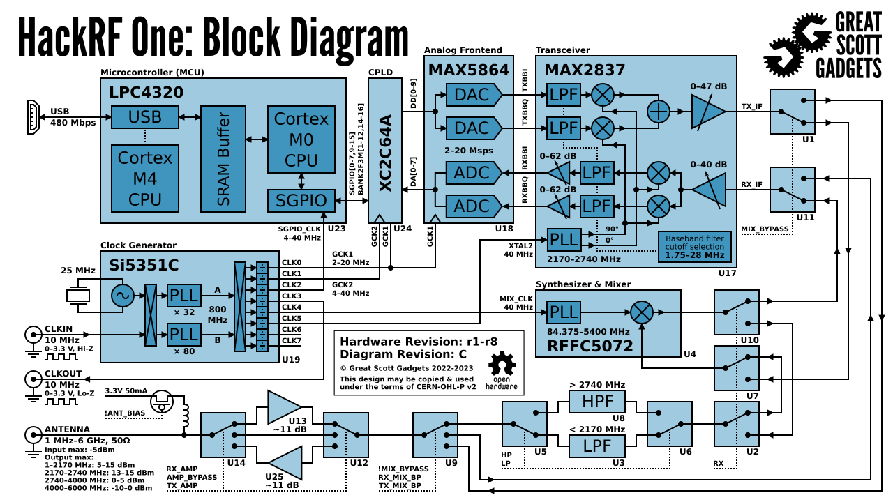
This diagram covers r1–r8. The linked design files are r10; r9 uses a different transceiver and clock arrangement. Check the revision notes before reusing a circuit.
1 board · Open hardware
From antenna to USB.
The RF front end shifts the signal into the transceiver’s range. The converters, CPLD and processor carry samples between the radio and your computer.
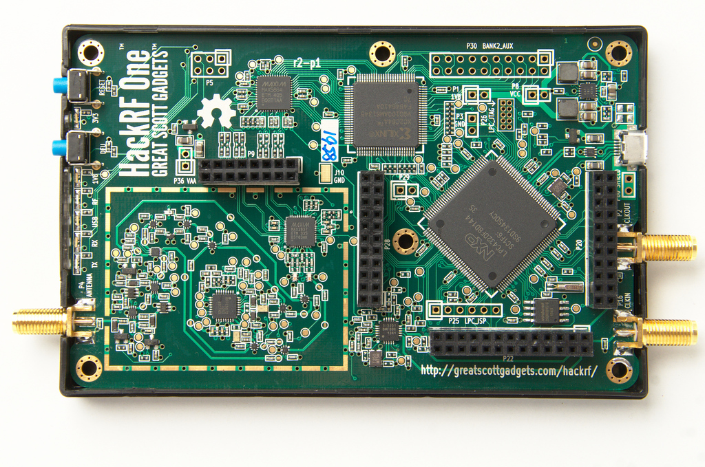
Early production hardware. Use the pinned r10 KiCad files for the current reviewed layout.
r10 source · earlier board pictured
Main PCB
The RF front end, sample converters and USB processor share a single board.
- LPC4320
- USB interface and sample buffering
- XC2C64A
- CPLD connecting the processor and converters
- MAX5864
- Analog-to-digital and digital-to-analog conversion
- MAX2837
- RF transceiver; r9 substitutes MAX2839
- RFFC5072
- Frequency mixer and synthesizer
- Si5351
- Clock generation; implementation varies by revision